Engineers are available to assist.

|
|
Edge Artificial Intelligence & Deep Learning |
|
|
Increases to Resolution Driving Innovation |
|
|
Event-Based Camera Technology |
|
|
Cost-Effective SWIR Imaging |
Rapid advancements in sensor and automation technology are bringing significant changes to the machine vision industry, optimizing industries such as manufacturing, healthcare, autonomous vehicles and robotics through artificial intelligence (AI), vision software, and novel hardware architecture. These changes increase productivity, cost savings, and improve decision-making capabilities in a number of applications across all industry spaces.
Edge AI, or edge learning, is a particular type of artificial intelligence that uses algorithms and deep learning neural networks directly with computing devices at the edge of a network. Data processing occurs primarily onboard the camera and information is exported directly to the connected cloud. These systems have the benefit of automating repetitive processes and operations for optimized power consumption, network latency, and increased overall application efficiency.
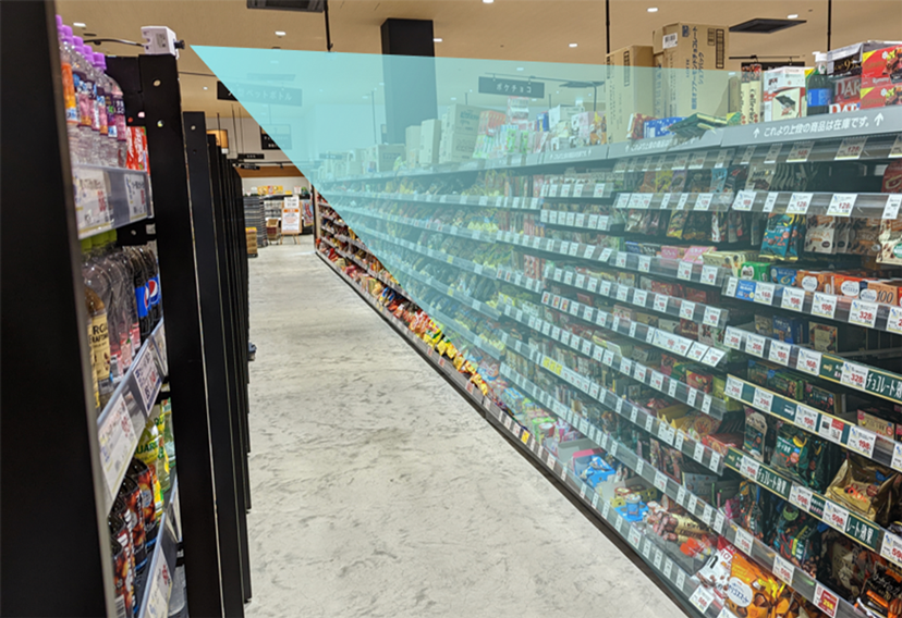
Figure 1: A LUCID Vision Labs™ SENSAiZ Intelligent Vision CMOS Camera keeps track of inventory levels at a convenience store and alerts personnel when supplies drop below a specified amount.
Artificial intelligence in and of itself is not a brand-new trend. Deep learning neural network models are being applied to applications at an increasing pace to achieve incredible results. What makes the LUCID Vision Labs™ SENSAiZ Intelligent Vision CMOS Camera different is the unique combination of high resolution with AI. Previous iterations of AI for machine vision utilized slightly lower resolution sensors, sampling the image at VGA resolutions.

Figure 2: The AITRIOS environment is a one-stop B2B platform that provides tools and an environment for application development and system integration. Image courtesy of Sony AITRIOS.
Lucid Vision Labs has partnered with Sony to pair the 12.33 Megapixel IMX500 machine vision camera sensor with the AITRIOS deep learning platform. Together, these technologies enable end users the ability to develop AI tools to increase application efficiencies, conserve resources such as power and bandwidth, and explore the frontiers of novel application spaces. Additionally, there are other camera manufacturers and software packages which accomplish similar goals including some Cognex camera models paired with the Vidi AI package.
Event-based machine vision, also known as neuromorphic vision, is an imaging method where the camera sensor, sometimes referred to as a dynamic vision sensor (DVS) takes a continuous record of exposure intensity, unobstructed by shutter. On a per pixel level, changes in intensity are recorded asynchronously and in a parallel manner similar to neural networks, conserving limited on-board computational resources.
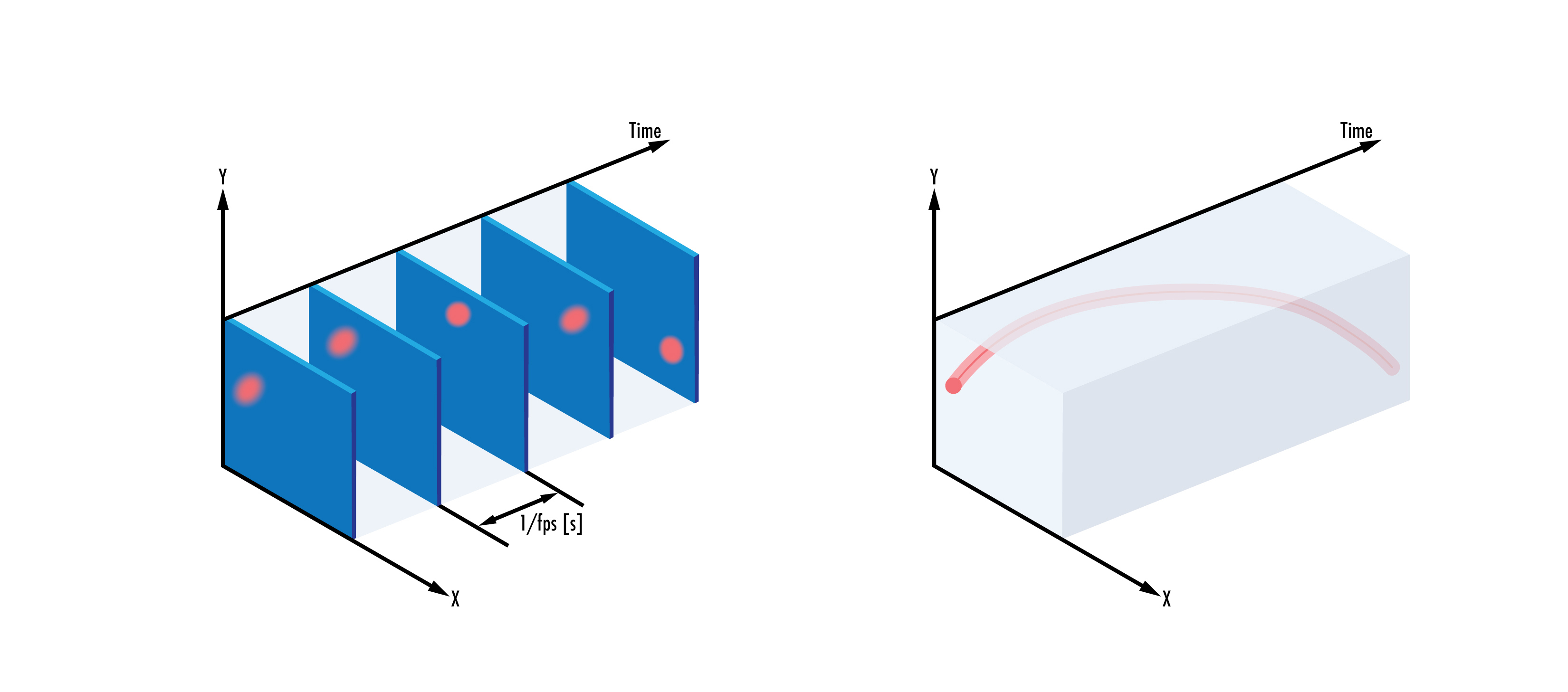
Figure 3: Conventional sensors (left) record frames at a fixed rate, independent of changes to the object in the field of view, whereas event-based sensors (right) capture changes to individual pixels depending on the detection of a change in intensity of the field of view.
Event-based imaging has low latency (on the magnitude of microseconds) and high temporal resolution, effectively eliminating frame rate altogether by capturing only essential motion information. Additionally, because of the elimination of frame rate, images have high dynamic resolution and low motion blur at low camera power consumption. This type of imaging has potential in robotics, autonomous vehicles, and many other industry spaces.
Short-wave infrared (SWIR) imaging uses light typically in the waveband between 0.9 and 1.7µm but can also include light from 0.7 to 2.5µm. Because SWIR wavelengths are outside of the visible spectrum and typical silicon sensors used for visible light are only sensitive to light up to around the near infrared spectrum (between 650nm and 1µm), SWIR sensors are constructed with other materials including indium gallium arsenide (InGaAs) and indium phosphide (InP). Traditionally, these sensors were very difficult to manufacture yielding high price points. However, advancements in SWIR sensor manufacturing techniques in the past few years have significantly improved manufacturing efficiency, and thus their affordability.
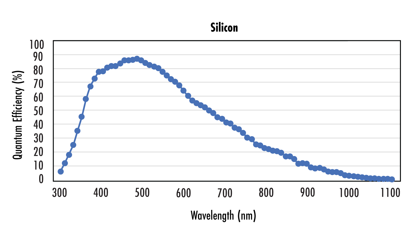
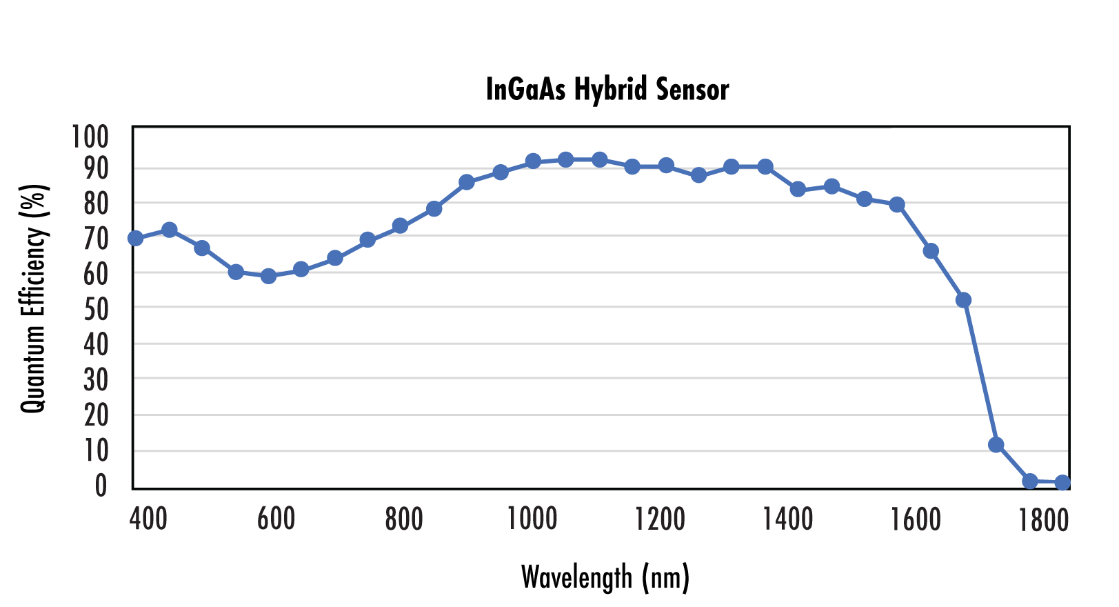
Figure 4: The quantum efficiency (QE) of traditional silicon (left) sensors is only sensitive to around 900nm to 1µm but InGaAs are sensitive out to much farther as seen in this visual-SWIR InGaAs hybrid sensor (right).
Previously steep price points for SWIR cameras created accessibility barriers to novel application adopters. As such, current applications using this technology are somewhat limited to agricultural and environmental monitoring, quality inspection for industrial applications including pharmaceuticals, and astronomy. With improved affordability, end users will be able to explore novel application spaces including art restoration and much more (Figure 5).
ROLL OVER to See SWIR Image


Figure 5: The Last Judgement by Jan Provost and imaged in the SWIR waveband by the Detroit Institute of Arts details the artist's original intention by carefully examining the underdrawing which lies beneath the paint film. Image copyright by Detroit Institute of Arts. Used with permission.


or view regional numbers
QUOTE TOOL
enter stock numbers to begin
Copyright 2023 | Edmund Optics, Ltd Unit 1, Opus Avenue, Nether Poppleton, York, YO26 6BL, UK
California Consumer Privacy Acts (CCPA): Do Not Sell or Share My Personal Information
California Transparency in Supply Chains Act
This content may include material that has been generated or modified using artificial intelligence (AI).
The FUTURE Depends On Optics®