Engineers are available to assist.


|
|
Back-lit vs. front-lit Illumination |
|
|
Sensor size increase and pixel size decrease for improved resolution |
|
|
Micro lenses for maximal light gathering |
|
|
New camera mount types for mechanical stability |
Over the last couple decades, advancements in mobile phone and smart phone camera technology have been at the forefront of developments in complementary metal-oxide-semiconductor (CMOS) technology. In turn, this has driven improvements to both the sensors and the methods for their fabrication. Also during this time, general manufacturing advancements have reduced noise in CMOS sensors and increased their reliability.
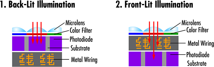
One specific alteration consisted of changing CMOS sensor structure from front-lit illumination to back-lit illumination.
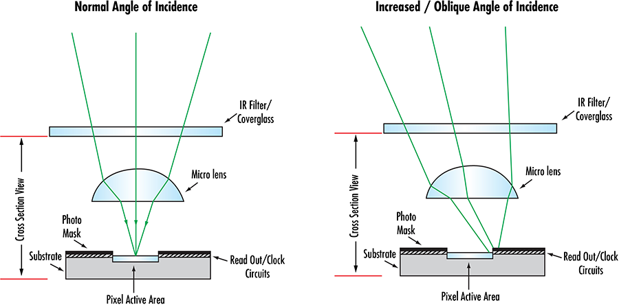
Another major improvement to the CMOS sensor design was the incorporation of micro-lenses to maximize the light capture to improve sensor efficiency.
After these years of technological advancements, the use of CMOS sensors has surpassed the use of charge-coupled devices (CCD) for several key reasons. CMOS devices are able to capture images while consuming less power than CCDs, and are less expensive to manufacture making them less expensive (by about a factor of 10) to purchase. By February 25, 2015, CMOS sensor technology was so popular that Sony announced it would cease production of CCD sensor technology.
As applications become more demanding, higher image quality and resolution are needed. CMOS manufacturers attempted to create sensors with higher resolutions by decreasing pixel size and increasing pixel counts. This was moderately successful; however, it came with some issues, including increased sensor noise. To combat this issue, manufacturers returned to slightly larger pixel sizes but on sensor formats larger than 1.1” sensor formats. This method increased sensor resolution and maintained good signal-to-noise ratios (SNR).
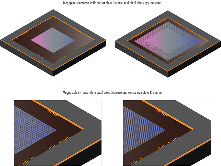
As resolution demands continue to increase, sensor manufacturers are not only making use of larger sensor formats but are also finding new ways to decrease pixel sizes without sacrificing image quality. One new sensor example is Sony’s 4th generation Pregius S 24.5 MP IMX530 CMOS, a 4/3″ sensor (diagonal 19.3mm) with a 2.74µm pixel size (37% smaller pixel size vs. 3.45µm).
However, as pixel sizes decrease and sensor sizes increase, significant changes to the optical designs must be made to make full use of increased performance. This requires imaging lens designs to incorporate additional optical elements, making imaging lenses larger in volume and heavier in weight. These two constraints put a strain on lens designers to create lenses with mounts larger than the C-mount and more robust and reliable than the consumer F-mount.
Lens mount types such as the TFL and TFL-II mounts feature compact flange distances and larger diameters for sensor formats like the APS-C, APS-H, and other full-frame sensors. These mounts are also threaded types that feature superior stability, support for heavy lenses, and alignment reliability over bayonet types like the F-mount.

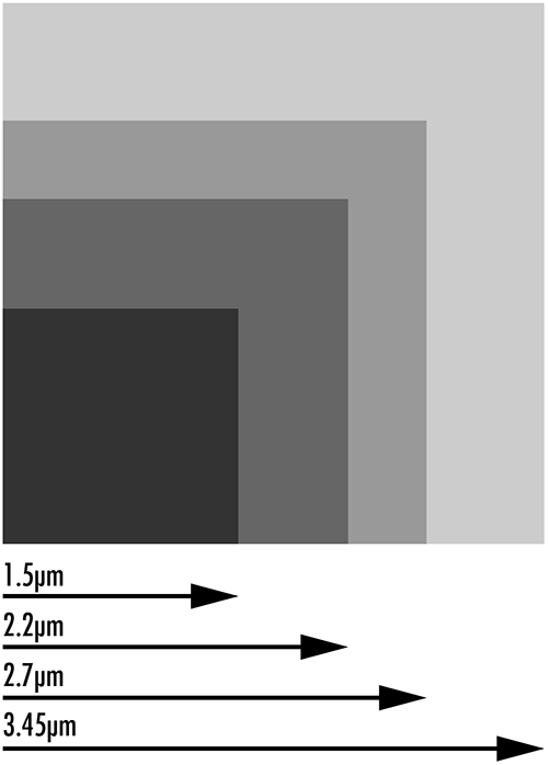
Sensor manufacturers are releasing the next generation of CMOS sensors with extremely high resolutions. The Canon 120MXS CMOS sensor features 120MP and pixels 2.2μm in size and the Canon 2U250MRXS CMOS features 250MP and pixels of 1.5μm. Both of these sensors have pixels with sizes much smaller than the industry’s typical pixel sizes. The new 4th generation of Sony Pregius sensors feature a smaller form-factor and an improved imaging performance of about 1.7X. These sensors also feature pixel sizes that have decreased from 3.45μm to 2.74μm.
As machine vision applications demand higher resolution, CMOS manufacturers will have to continue reducing the size of individual pixels and increasing the overall size of sensors to improve image quality and effective resolution.
 Does Edmund Optics sell cameras with a TFL Mount?
Yes, Edmund Optics has partnered with LUCID Vision Labs to offer the ATLASTM camera family.
Which imaging lenses feature a TFL Mount?
The TECHSPEC® CA Series Fixed Focal Length Lenses feature a TFL Mount and have been designed specifically for new large sensor formats.
Which imaging lenses feature a TFL-II Mount?


or view regional numbers
QUOTE TOOL
enter stock numbers to begin
Copyright 2023 | Edmund Optics, Ltd Unit 1, Opus Avenue, Nether Poppleton, York, YO26 6BL, UK
California Consumer Privacy Acts (CCPA): Do Not Sell or Share My Personal Information
California Transparency in Supply Chains Act
This content may include material that has been generated or modified using artificial intelligence (AI).
The FUTURE Depends On Optics®